 牛津仪器集团成员

半导体是当代科技的基石,推动了计算、通信、能源和光电子等领域快速发展。从晶体管到光伏和LED,半导体材料是无数设备的核心。为了满足对性能、效率和可靠性日益增长的需求,在从研发到生产的每个阶段,半导体性能的精确表征至关重要。
共焦拉曼显微镜和光致发光(PL)成像技术是半导体研究的强大工具,能够提供化学结构和电子性质等重要信息。这些分析必将助力半导体研发与企业的质量控制,生产流程优化,并加速新设备上市时间。
WITec alpha300 系列配备了最先进的拉曼和 PL 测量功能,可在一台仪器中完成测量,为半导体领域提供先进的解决方案。alpha300 显微镜都能帮助研发人员或制造商全面了解材料,包括材料均匀性和半导体能带分析,进而突破半导体创新中的挑战和困难。
对于全晶圆分析,我们发布了专门的 alpha300 半导体版,该版本针对大面积成像优化,可容纳最大 12 英寸(300 毫米)晶圆。
alpha300 半导体版
拉曼成像与PL成像可实现关联分析,为研究人员和制造商提供材料性能和器件质量分析的直接证据。
更多信息可以参考我们的应用案例《化合物半导体相关拉曼成像》,了解在晶圆分析中进行相关拉曼-PL测量示例。
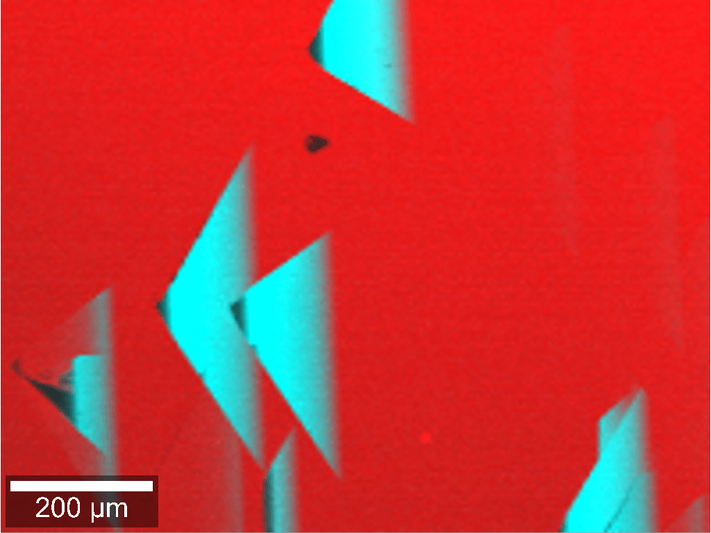
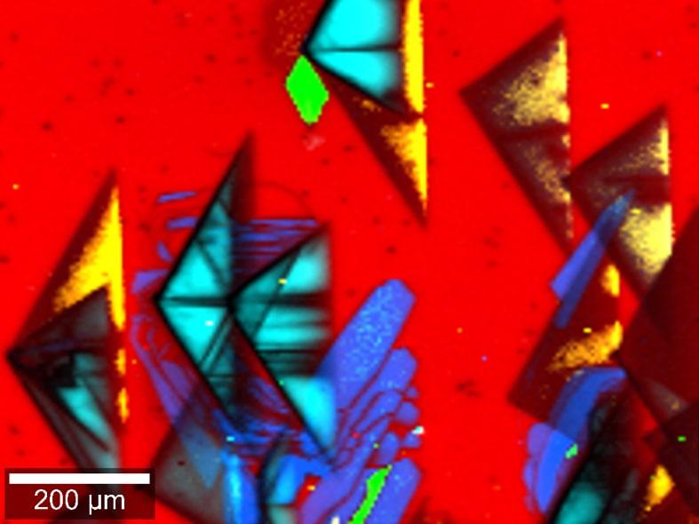
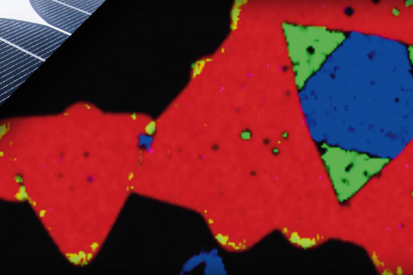
半导体晶体结构中的微小变化(例如由应力或应变引起的)可能会对其稳定性和电学性能带来极大地影响。WITec alpha300 拉曼显微镜具有卓越的灵敏度,能够准确分辨出微小的拉曼峰位移,精度可达波数的十分之一或百分之一。以氮化镓 (GaN) 为例,我们能够识别出由弗兰克-里德源引起的拉伸应力场(蓝色和绿色区域)。
如需了解更多关于材料应力分析的详情,请参阅我们的应用案例《化合物半导体相关拉曼成像》。


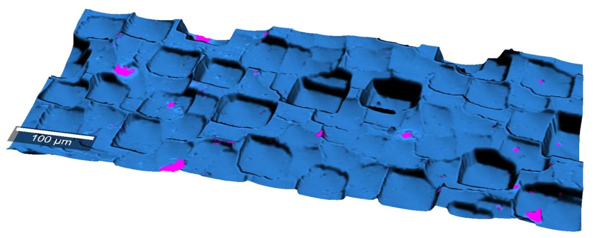
共焦拉曼显微镜可实现半导体材料的无损亚表面结构分析。沿xz平面进行的拉曼深度分析是确定晶圆内掺杂分布的理想方法,同时保持样品完整性。
在此示例中,拉曼深度成像成功分辨了掺杂后的 4H-SiC 晶圆中不同掺杂浓度的层:基板(蓝色)、1 µm 中间缓冲层(绿色)和 9 µm 外延层(红色)。凭借 alpha300 卓越的共焦性,才能获得准确获得这些薄膜的层相对厚度的重要信息。
如需了解更多详情,请参阅我们的应用案例《化合物半导体相关拉曼成像》。
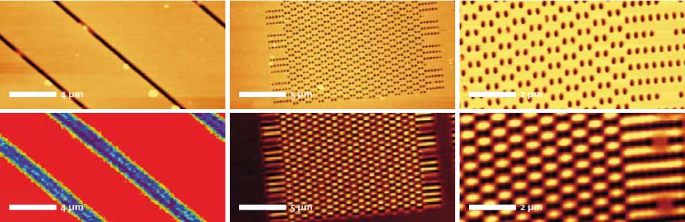
在晶圆大范围成像中,如何使共焦拉曼成像在结构化表面上保持聚焦?
实时聚焦TrueSurface专利技术完美解决了这一问题。在大晶圆拉曼测试中,TrueSurface会持续追踪聚焦平面以适应晶圆翘曲的不平,从而在成像中保持卓越的拉曼聚焦稳定性。不仅如此,TrueSurface 还可在同步提供晶圆表面轮廓图像和测量数据。
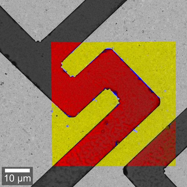
将拉曼成像与其他先进的成像分析技术相结合,有助于更深入地探索半导体材料的性能。WITec alpha300 显微镜的关联分析方法可将各种技术无缝整合,分析化学成分、电学性能、表面翘曲、元素分布,并获取高分辨率的结构数据。这有助于全面了解半导体材料,从而优化半导体材料生长或加工工艺,以满足尖端应用的需求。

© 牛津仪器 2026
 公安机关备案号31010402003473